About Us

Pioneering Semiconductor Innovation

Advancing India's semiconductor capability through innovation, technical excellence, and industry collaboration.

VLSI Layout Design
Our Story

India's Pioneer in Integrated Silicon Ecosystems

Vayuvyastra Semicon is an Indian deep-tech startup with a bold national mission: to establish India's first comprehensive in-house semiconductor design, wafer fabrication, and manufacturing ecosystem under a single roof. Our flagship program represents a ₹1,90,000 Crore investment spanning 12 years and four strategic phases (2025–2037).

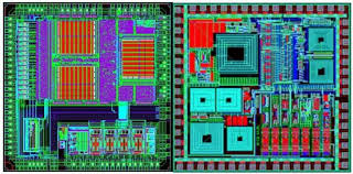
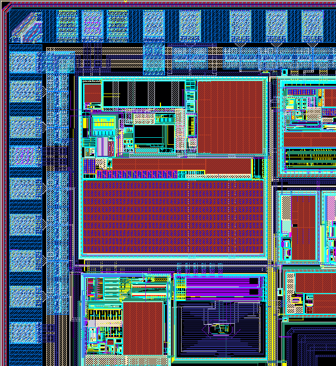
Operating from an integrated 4,000-acre campus, our facilities host advanced wafer fabs processing nodes from 65nm down to 5nm, Class 1-100 cleanrooms, R&D centers, an employee township, and three dedicated downstream assembly plants. Our journey is driven by anchoring India's technological sovereignty in the 21st century.

By producing chips locally and packaging them into high-value modules, we directly address India's 85%+ import dependency, which generates a $30+ Billion annual trade deficit. Vayuvyastra Semicon positions India as a Tier-1 global semiconductor exporter and secures national supply chains against geopolitical risks.

Meet Our Leadership
Our Foundation

Mission, Vision & Values

Guiding principles that drive our pursuit of national semiconductor sovereignty and technical excellence.

Our Mission

Build India's most comprehensive in-house semiconductor design, fabrication, and downstream assembly ecosystem, reducing import dependency and ensuring first-silicon success.

Our Vision

To be a Tier-1 global semiconductor manufacturer and exporter, anchoring India's technological sovereignty and powering international technology supply chains.

Core Values

Silicon Sovereignty • R&D Driven Innovation • Quality (Class 1-100 Discipline) • Geopolitical Resilience • Nation Building — guiding our mega-fab execution.

Our Approach

Industry-Grade Engineering

We follow global semiconductor best practices, ensuring our processes and outputs meet the highest industry standards. Our approach is modeled after leading semiconductor companies worldwide.

Structured Engineering Workflow

Systematic approach from concept to silicon

Semiconductor-Grade Quality

Rigorous quality control at every stage

Performance-Driven Execution

Focus on optimal results and efficiency

Strong Reliability Mindset

Building products that perform consistently

Chip Layout Design
Trust & Recognition

Certifications & Policy Alignment

Building credibility through recognized certifications, standard alignments, and government policies.

Active Certifications & Credentials

ISO Certified
MSME Registered
DPIIT Recognized Startup
T-Hub Hyderabad

Strategic Fabs & Policy Alignment

MeitY ISMC Scheme Partner
India Semiconductor Mission
State PLI (Telangana/AP Model)
US DoD & EU Chips Act Trusted Fab
Geopolitical Resilience

Geopolitical Resilience & The Indian Semiconductor Challenge

Establishing India's silicon sovereignty and securing high-tech supply chains against global disruptions.

India's Semiconductor Problem: Current Impact vs. Vayuvyastra's Solution

Vulnerability / Parameter Current National Impact Vayuvyastra's Strategic Solution
85%+ Import Dependency ₹2,50,000 Crore annual foreign exchange outflow. In-house wafer fabrication, targeting zero-import for covered process nodes.
No Advanced Fab (Below 28nm) AI, 5G, and high-performance computing chips are 100% imported. Scaling to 5nm FinFET/GAA transistor nodes by Phase IV.
China Supply Vulnerabilities Critical LED modules and CCTV chip supply chains frequently disrupted. Integrated domestic LED packaging and CCTV SoC manufacturing lines on campus.
US-China Tech War Impact Export controls and tool/IP access uncertainty for domestic buyers. Multi-country supply network (US, EU, Japan) combined with proprietary IP library ownership.
No Local Defence-Grade Source Strategic/DRDO systems rely on imported chips, risking geopolitical delays. Dedicated radiation-hardened and mil-grade fabrication processes.
Healthcare Device Chip Gap 85% of medical diagnostic and life-saving equipment relies on imported chips. ISO 13485 certified Healthcare Electronics Unit online in Phase I.

Cost & Lead-Time Advantages

Reduced Lead Times

Current global lead times exceed 26–52 weeks from foreign fabs. Vayuvyastra targets domestic turnarounds of just 4–6 weeks at scale.

Lower Landed Costs

Indian companies pay a 15–40% logistics, duty, and premium markup on imports. Domestic production yields 20–30% lower pricing.

Zero Currency Risk

Contracts denominated entirely in Indian Rupees (INR) protect domestic OEM buyers from US Dollar and Euro exchange rate volatility.

Why Vayuvyastra Semicon

What Sets Us Apart

Key differentiators that make Vayuvyastra Semicon your ideal semiconductor partner.

T-Hub Advantage

Operating from India's leading innovation hub with access to ecosystem resources.

Expert Team

Industry veterans with deep expertise in semiconductor and embedded systems.

Innovation Focus

R&D driven approach with continuous investment in emerging technologies.

Partnership Model

Collaborative engagement focused on mutual success and long-term value.

Partner with Vayuvyastra Semicon

Join us in building India's semiconductor future. Let's create innovative solutions together.